
October 20-23, 2026
EuroNanoLab Experts School

Keynote Speakers
-

Chris A. Mack
Chief Technical Officer
Fractilia -

Elena Pinilla-Cienfuegos
Associate Professor at the Universitat Politècnica de València (UPV)
-

Jordi Llobet
Researcher at the Institute of Microelectronics of Barcelona (IMB-CNM-CSIC)
-

Karen Birkelund
Head of lithography and wet chemistry atTechnical University of Denmark (DTU) | DTU Nanolab | National Centre for Nano Fabrication and Characterization
-

Helmut Schift
Head of the Polymer Nanotechnology Group in the Laboratory for Micro- and Nanotechnology at the Paul Scherrer Institut
-
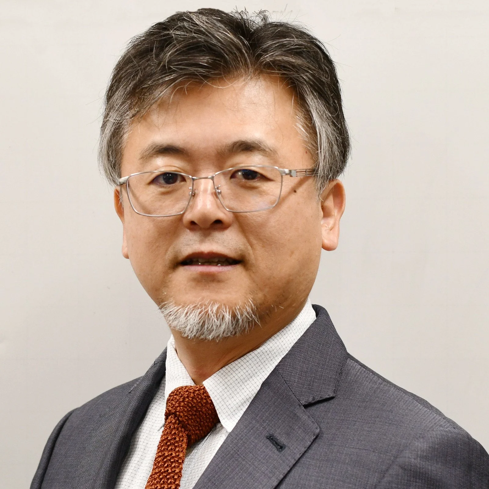
Yoshio Mita
Full professor of the Department of Electrical Engineering and Information Systems (EEIS)
Invited Speakers
-

Andreas Gejl Madsen
Researcher and engineer at the Syddansk Universitet (SDU in Denmark)
-
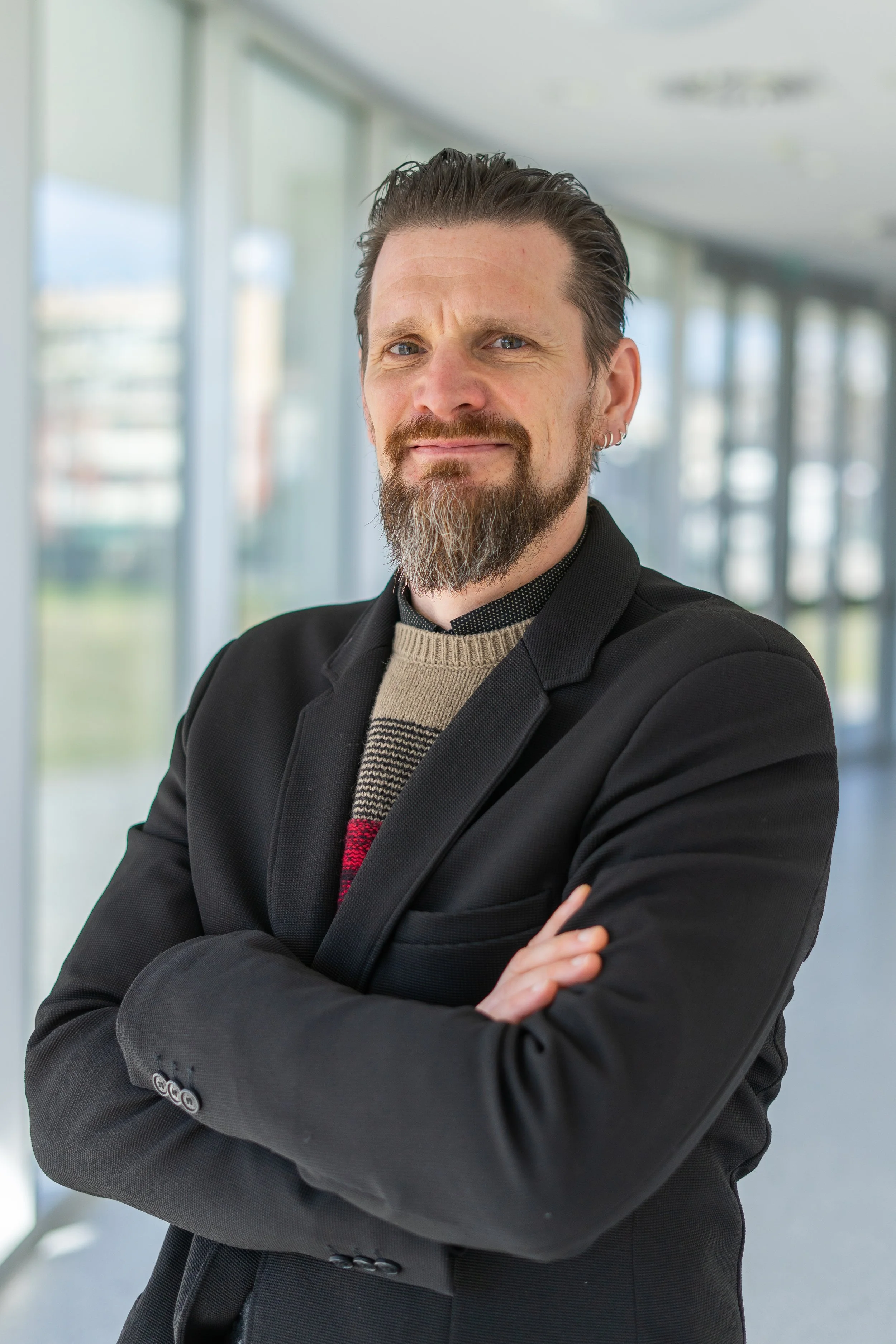
Christian Maibohm
Research Scientist at the International Iberian Nanotechnology Laboratory
-

Bhavishya Chowrira
Senior R&D Engineer at imec
-

Diogo Aguiam
Staff Researcher at the International Iberian Nanotechnology Laboratory
-

Douglas Guerrero
Technology strategy and management, Brewer Science, Inc
-

Eliott Clerc
R&D Engineer in the Process and Applications Laboratory at Heidelberg Instruments Nano
-
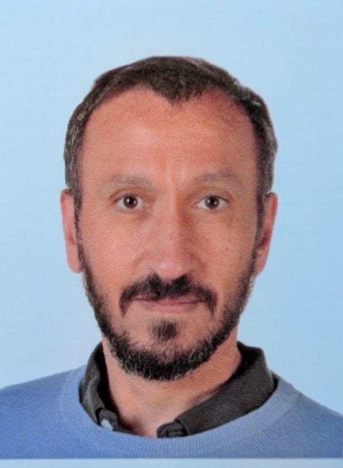
Gianluca Grenci
University of Padua
-

Jan Beltman
Manager Applications Mature Products at ASML
-

Jens Hemmingsen
Technical University of Denmark (DTU)
-
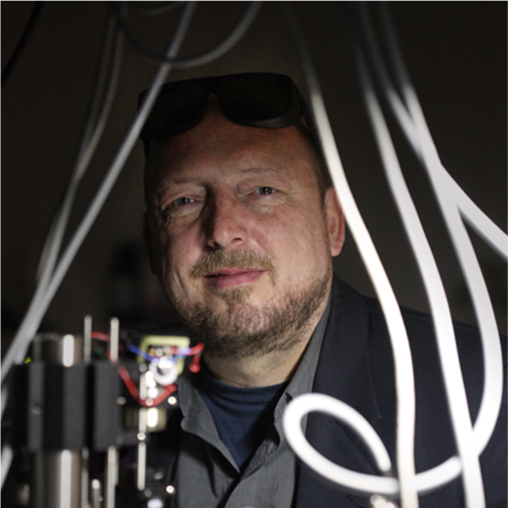
Jesper Glückstad
Professor & Head of SDU Photonics Engineering, Univ. Southern Denmark
-
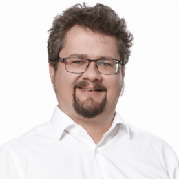
Jochen Zimmer
3D microfabrication expert and Sales Manager at Nanoscribe
-
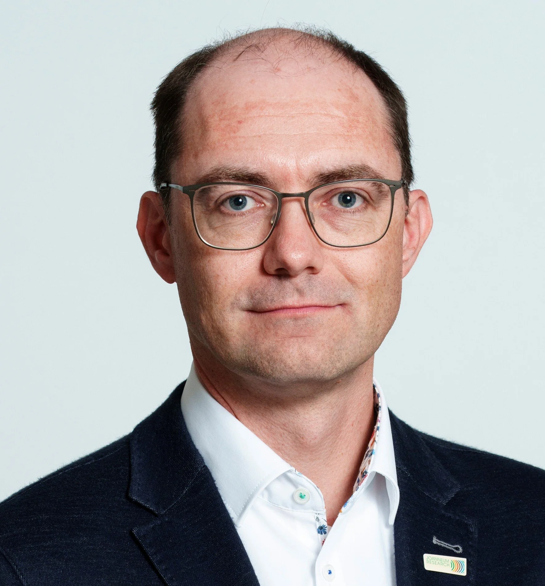
Markus Postl
JOANNEUM RESEARCH
-
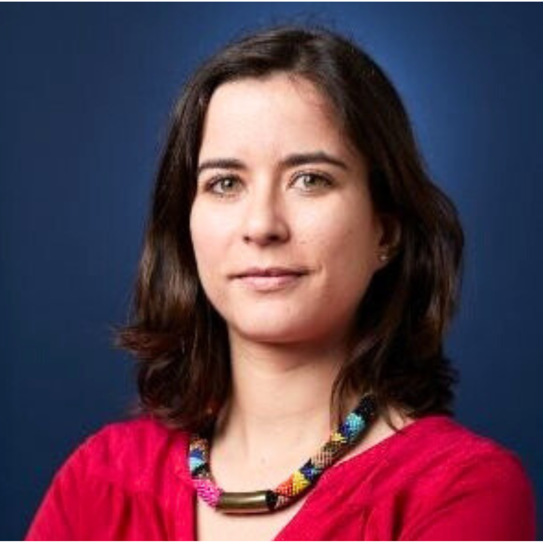
Rita Macedo
INESC-MN
-
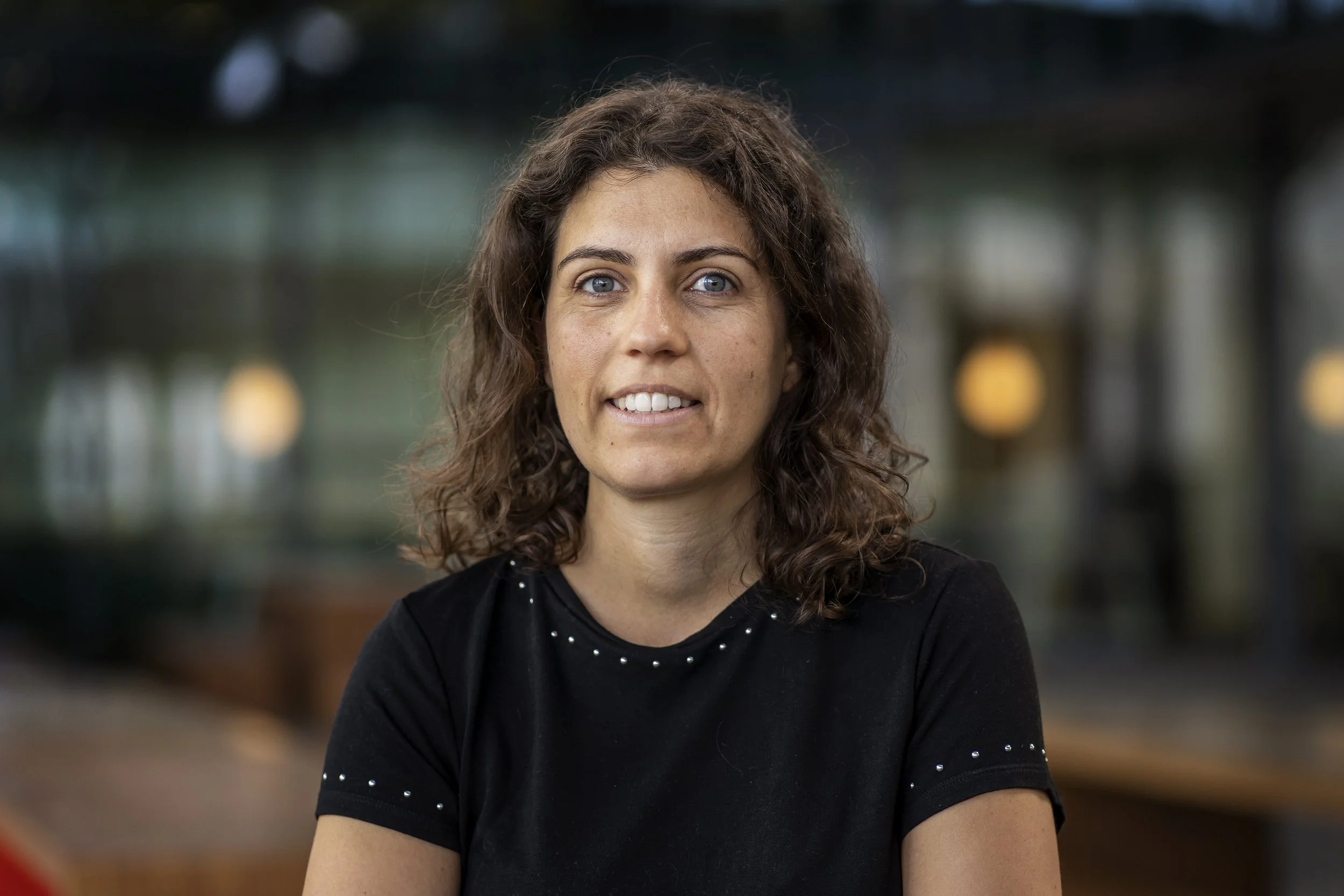
Sara Sequeira
Eindhoven University of Technology
-

Saulo Moura
Applications Engineer Mature Products at ASML
-

Søren Isaksen
CEO of Copenhagen Microsystems
-
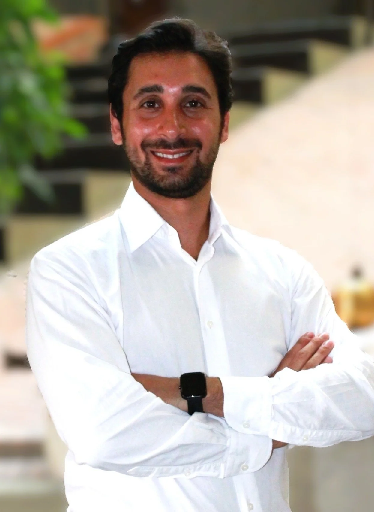
Stefano L. Oscurato
Professor & Lead of Holo-Lithography Research Group at the Department of Physics “Ettore Pancini”, University of Naples Federico II
-
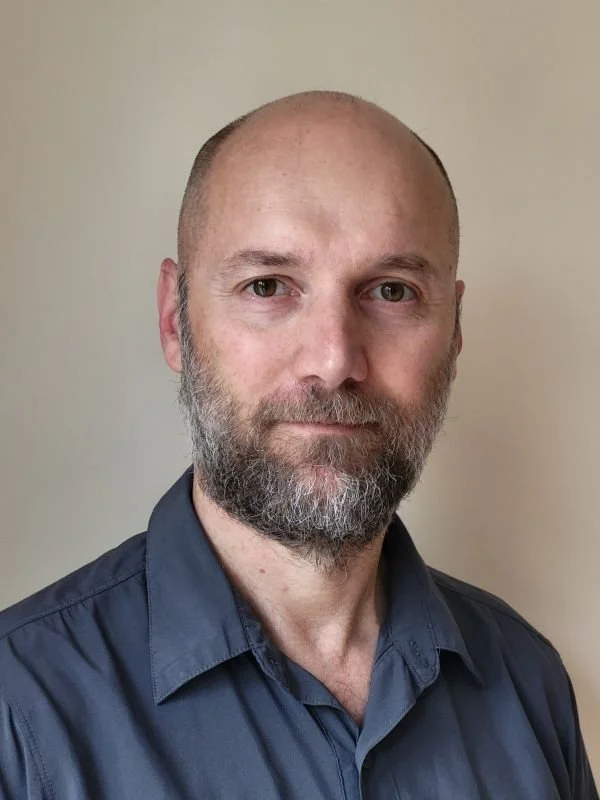
Vincenzo Miceli
Senior Staff Engineer
Lithography Yield Improvement Lead & Advanced Overlay Specialist, Intel Corporation -

Yu Kyoung Ryu
Instituto de Sistemas Optoelectrónicos y Microtecnología (Universidad Politécnica de Madrid)
-
Yann Chevolot
CNRS, École Centrale de Lyon
Who should attend?
This event welcomes the entire European nanotechnology community and beyond:
Academic researchers seeking to expand their expertise or discover new techniques
Industry professionals driving innovation in nanofabrication
Cleanroom managers and technical experts wanting to strengthen their competencies
Anyone passionate about the future of micro- and nanotechnology
PhD students and early-career researchers exploring lithography technologies

Why Attend?
Learn from leading experts in lithography across Europe's premier nanofabrication centres
Explore emerging technologies, including nanoimprint lithography, interference lithography, and sustainable materials
Build your professional network with researchers and industry partners across the European nanotechnology ecosystem
Access world-class facilities through exclusive cleanroom tours
Be part of a growing movement toward green and sustainable nanofabrication practices
Gain hands-on experience with cutting-edge techniques and equipment
Register now to secure your place in this inaugural event.
Spaces are limited, particularly for hands-on training sessions and cleanroom tours. All participants are eligible to receive a certificate of participation. Please indicate your preference during registration.
Deadline: October 16

Poster Presentation
Participants are invited to present a poster during the school. All poster presenters will receive a certificate of presentation.
Submission Guidelines
Abstracts must be written in English and must not exceed 2,500 characters including spaces
Format: A0 (841 × 1189 mm), portrait orientation
Posters may be displayed in the designated poster area following check-in
Deadline & Selection
Submit your abstract by September 30, 2026. All submissions will be reviewed by the Organising Committee, and applicants will be notified of the decision via the email address provided at submission.

Building European Excellence in Nanofabrication
The inaugural Lithography Experts School marks a major milestone for the EuroNanoLab consortium, establishing a premier platform to advance lithography expertise across Europe. This foundational event strengthens the four core pillars that define our mission:

Enhance excellence by building superior processing competence in advanced lithography techniques.
Share competencies by defining European standards in cleanroom procedures and lithography best practices.
Accelerate research by enabling process exchange and providing a single access point to micro- and nanofabrication research infrastructure and expertise.
Strengthen cooperation by building an alliance between scientists and micro- and nanofabrication experts.
Expert-Led Education and Knowledge Exchange
Internationally recognised academic and industrial lithography specialists will deliver lectures covering the full spectrum of modern lithography: from fundamental principles and resist chemistry to advanced patterning techniques, process simulation, and cutting-edge applications across multiple technology nodes.
The school creates a dedicated space for lithography experts to connect, exchange ideas, discuss recent breakthroughs and technical challenges, and explore emerging advances in lithography equipment and processing technologies. By bringing together the European nanofabrication community, the 1st Lithography Experts School establishes a foundation for sustained collaboration and accelerated innovation in one of the most critical technologies for next-generation device fabrication.
The EuroNanoLab Expert School Lithography is the flagship educational initiative from our network, bringing together researchers, PhD students, early-career scientists, and industry professionals to explore the present and future of lithography technologies. This inaugural school represents our commitment to fostering excellence in nanofabrication through hands-on training and knowledge exchange.
Over four intensive days in Braga, Portugal, participants will engage with:

Foundational & Advanced Techniques: Optical, laser, and electron-beam lithography
Hands-On Training: Limited-capacity sessions designed for non-expert participants to build practical skills.
Cutting-edge Approaches: Nanoimprint lithography (NIL), interference lithography, greyscale, and emerging alternative techniques.
Cleanroom Tours: Expert-led facility tours showcasing world-class nanofabrication infrastructure.
Sustainability Focus: Green materials and sustainable practices in lithography.
Networking & Collaboration: Direct engagements with leading lithography experts and peers across Europe's nanotechnology ecosystem.
Our sponsors





Gold

Local supporters

TUESDAY - OCTOBER 20
| Time | Title | Presenter |
|---|---|---|
| 08:30 | Welcome to INL with coffee/tea | |
| 09:00 | School opening ceremony | TBD |
| 09:45 | EuroNanoLab organisation | TBD |
| 10:30 | Coffee break | |
| 11:00 | Talk #1 | TBD |
| 11:45 | Talk #2 | TBD |
| 12:30 | Lunch buffet | |
| 13:30 | Talk #3 | TBD |
| 14:15 | Talk #4 | TBD |
| 15:00 | Coffee break | |
| 15:30 | Talk #5 | TBD |
| 16:15 | Talk #6 | TBD |
| 17:00 | Cleanroom tours | |
WEDNESDAY - OCTOBER 21
| Time | Title | Presenter |
|---|---|---|
| 08:30 | Coffee/tea | |
| 09:00 | Talk #7 | TBD |
| 09:45 | Talk #8 | TBD |
| 10:30 | Coffee break | |
| 11:00 | Talk #9 | TBD |
| 11:45 | Talk #10 | TBD |
| 12:30 | Lunch buffet | |
| 13:30 | Talk #11 | TBD |
| 14:15 | Talk #12 | TBD |
| 15:00 | Coffee break | |
| 15:30 | Talk #13 | TBD |
| 16:15 | Talk #14 | TBD |
| 17:00 | Cleanroom tours | |
| 18:00 | Free time | |
| 19:00 - 22:00 | School dinner | |
THURSDAY - OCTOBER 22
| Time | Title | Presenter |
|---|---|---|
| 08:30 | Coffee/tea | |
| 09:00 | Talk #15 | TBD |
| 09:45 | Talk #16 | TBD |
| 10:30 | Coffee break | |
| 11:00 | Talk #17 | TBD |
| 11:45 | Talk #18 | TBD |
| 12:30 | Lunch buffet | |
| 13:30 | Talk #19 | TBD |
| 14:15 | Talk #20 | TBD |
| 15:00 | School closing ceremony | TBD |
| 15:30 | Coffee break | |
| 16:15 | Cleanroom tours | |
| 17:00 | Cleanroom tours | |
FRIDAY - OCTOBER 23
| Time | Title | Presenter |
|---|---|---|
| 08:30 | Coffee/tea | |
| 09:00 | Students hands-on training | MNF staff |
| 09:45 | Students hands-on training | MNF staff |
| 10:30 | Coffee break | |
| 11:00 | Students hands-on training | MNF staff |
| 11:45 | Students hands-on training | MNF staff |
| 12:30 | Lunch buffet | |
| 13:00 | Farewell | TBD |
Preliminary Programme
What is EuroNanoLab?
EuroNanoLab is a distributed research infrastructure uniting more than 40 state-of-the-art academic nanofabrication centres across Europe. Our mission is to accelerate research in micro- and nanotechnology by transforming a fragmented landscape of national facilities into an integrated, collaborative knowledge base that drives scientific excellence and innovation.
As a collective of leading European cleanrooms, EuroNanoLab offers a single point of access to cutting-edge expertise, world-class equipment, and shared knowledge — enabling researchers, students, and industry partners to achieve breakthroughs faster and more efficiently.
EuroNanoLab strives to provide:
New nanofabrication systems capable of fabricating more complex micro- and nanodevices, by integrating the specialised contributions of multiple cleanrooms to accelerate high-impact scientific projects.
Coordinated user access to world-class nanofabrication equipment, expertise, technology development, and a shared knowledge base through a central hub.
Multidisciplinary outreach and novel nanofabrication building blocks, co-defined with leading experts across key scientific communities: quantum technologies, 2D materials, nanobiosciences, neuromorphic computing, and astronomy and space exploration.
Fast technology transfer to start-ups and SMEs.
EuroNanoLab contributes to innovative solutions for societal challenges in energy, environment, transport, health, and general well-being. Achieving ESFRI landmark status will further strengthen EuroNanoLab's recognition at both national and international levels.
EuroNanoLab's model draws inspiration from the NNIN — the US distributed infrastructure of academic cleanrooms established in 2004. EuroNanoLab’s core partners include cleanroom networks that have been working with this model for over 15 years (Sweden, the Netherlands, France, and Norway).
-
Expanding Access to Nanofabrication Innovation Across Europe
Scientists pursuing exploratory research, whether from academic institutions or industry, naturally tackle diverse and novel challenges. This means their requests to nanofabrication facilities often come with unexpected requirements, and even Europe's most advanced cleanrooms cannot stock every specialised process needed to meet every researcher's demands. Developing new processes to address these gaps typically requires lengthy, uncertain timelines.
Yet the missing capabilities frequently exist elsewhere: across Europe's distributed network of cleanrooms, ready-made solutions sit unused because neither the facilities nor the researchers know they're available. A well-coordinated European infrastructure could unlock this hidden potential, offering researchers access to a far richer toolkit of process expertise than any single centre could provide alone. By connecting researchers with the right capabilities, wherever they're located, EuroNanoLab can deliver faster, higher-quality solutions to nanofabrication challenges that might otherwise require months of development.
-
Build a Europe-wide nanofabrication infrastructure capable of providing university/industrial users with manufactured nano-objects for research with the highest quality and fastest delivery time.
Work jointly with European-wide research communities (e.g., flagship or other initiatives) to support their research by anticipating the development of appropriate new technologies.
-
-
-

Scientific and Organisational Committees
-

José Rodrigues
Micro and Nanofabrication Facility Lead
International Iberian Nanotechnology Laboratory
-
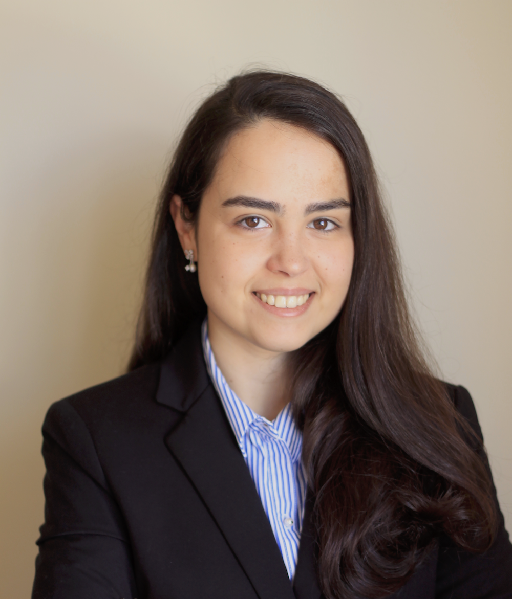
Joana Santos
Micro and Nanofabrication Facility Engineer: Lithography Specialist
International Iberian Nanotechnology Laboratory
-
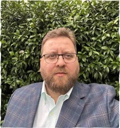
Ivan Prieto
Head of Micro and Nanofabrication Facility
International Iberian Nanotechnology Laboratory
-
Laurent Mazenq
Engineer / Coordination support for the EuroNanoLab Litho Expert Group
LAAS-CNRS (FR)
-
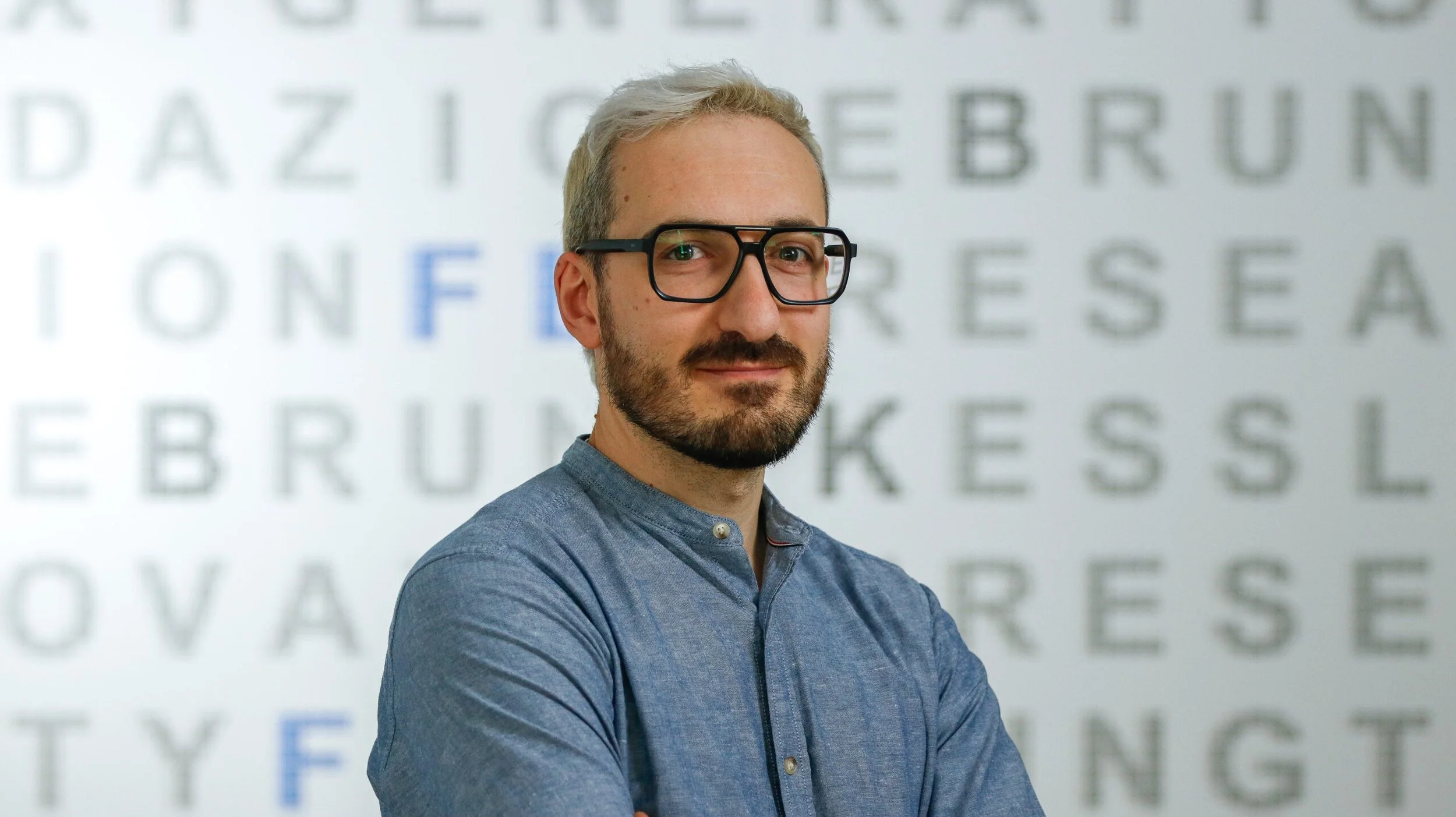
Alessandro Cian
Researcher / Coordination support for the EuroNanoLab Litho Expert Group
Fondazione Bruno Kessler (IT)
-

Mario Malerba
Researcher / Coordination support for the EuroNanoLab Litho Expert Group
National Metrology Institute of Italy (IT)
-

Nathalie Bardou
Engineer / Coordination support for the EuroNanoLab Litho Expert Group
C2N-CNRS (FR)
Accommodation
Braga offers a range of accommodation options to suit different budgets and preferences.
We have compiled a selection of recommended hotels and guesthouses conveniently located near the venue. For the full list and booking details, please visit our accommodation page.
Venue
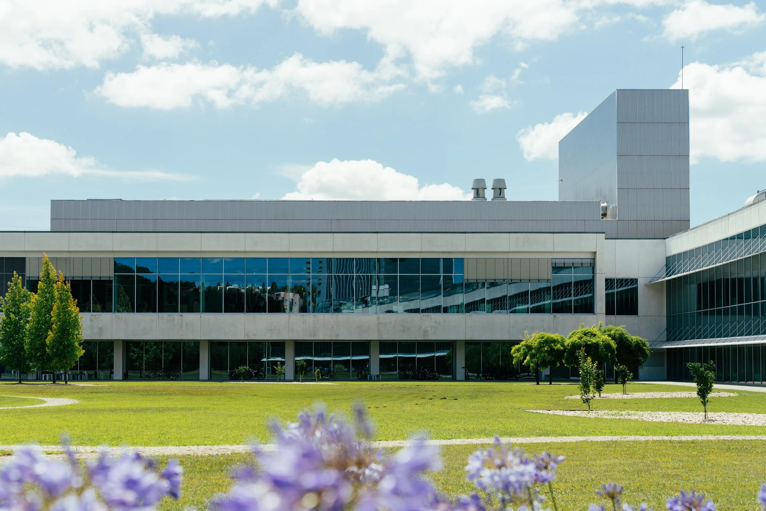
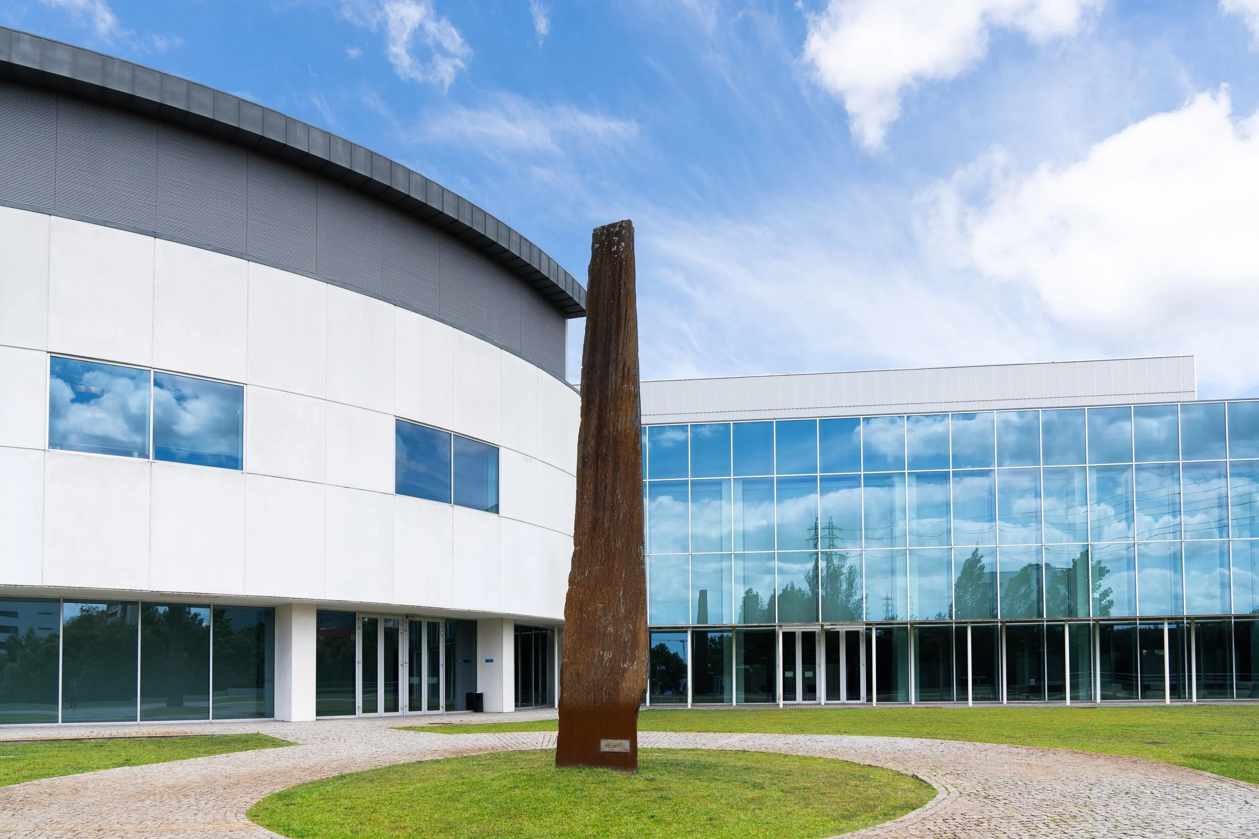
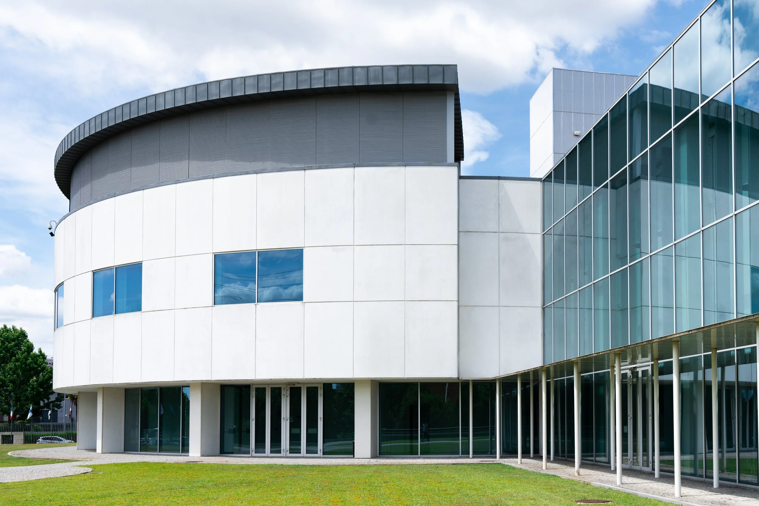
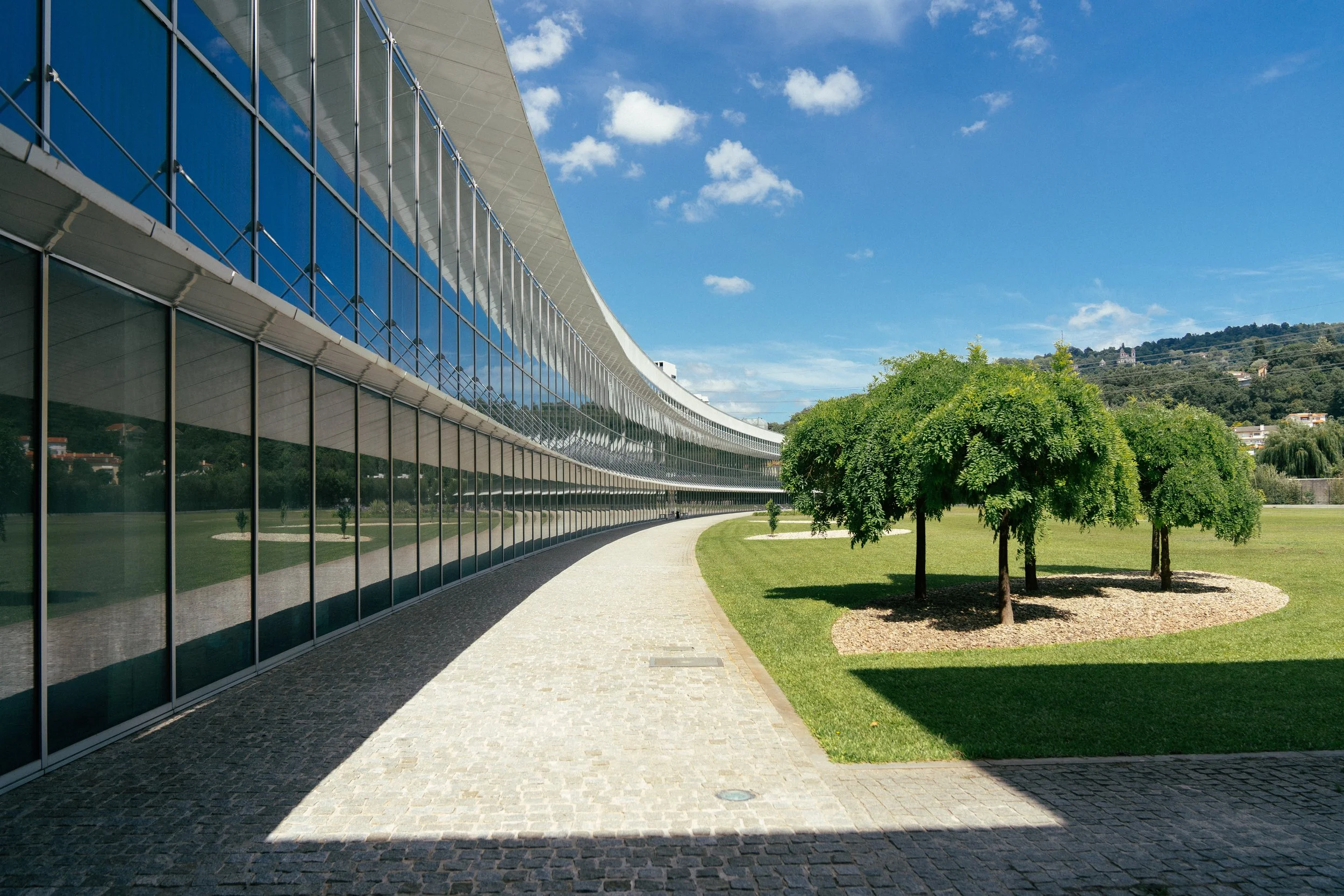
The INL International Iberian Nanotechnology Laboratory, located in Braga (North of Portugal), was founded by the governments of Portugal and Spain under an international legal framework to perform interdisciplinary research and deploy and articulate nanotechnology for the benefit of society.
INL aims to become the worldwide hub for nanotechnology, addressing society’s grand challenges.
INL – International Iberian Nanotechnology Laboratory
Av. Mestre José Veiga
4715-330 Braga | Portugal
Let’s talk!
For any queries, please contact the Conference Team. Fill in the form, and we will be in touch soon!
INL – International Iberian Nanotechnology Laboratory
Av. Mestre José Veiga
4715-330 Braga | Portugal