Title:
Beyond the Golden Tool: Leading-Edge EUV Patterning Challenges in High-Volume Manufacturing
Abstract:
Transitioning leading-edge Extreme Ultraviolet (EUV) lithography from a development environment to 24/7 High-Volume Manufacturing (HVM), shifts the engineering paradigm from single-wafer feasibility to statistical predictability, tool availability, and strict cost of ownership. While Technology Development (TD) relies on small scanner fleets and custom per-wafer optimizations, HVM demands absolute fleet interchangeability across dozens of exposure systems to deliver predictable yield and performance across thousands of wafer starts per week.
This presentation examines the critical physical, operational, and economic bottlenecks encountered when scaling EUV patterning to mass production. Key topics include:
Fleet Availability and Output: Managing fleet uptime, tool speed, scheduled maintenance, source power degradation, collector mirror lifetime, and the acute trade-off between exposure dose and scanner throughput (WPH).
Cross-Tool Matching & Advanced Process Control (APC): Controlling high-order overlay and maintaining machine-to-machine overlay (MMO) matching across both EUV and DUV platforms via closed-loop feedback.
Dimensional Control & Stochastics: Mitigating slit-dependent 3D mask effects, inter-tool critical dimension uniformity (CDU), and parts-per-billion stochastic defectivity.
Rework & Reticle Management: Addressing the high costs and material risks of rework, ensuring reticle integrity and defect-free printing, and managing pellicle durability under high source power.
Sustaining Operations & Vendor Ecosystem: Structuring 24/7 fab engineering models and leveraging joint co-development with scanner, track, resist, and metrology suppliers.
Attendees will gain an insider’s perspective on how HVM factories operate, the real-world manufacturing constraints they face, and the engineering required to solve the ultimate challenge of leading-edge lithography: patterning billions of nanometer-scale features identically, flawlessly, and economically in large volumes.
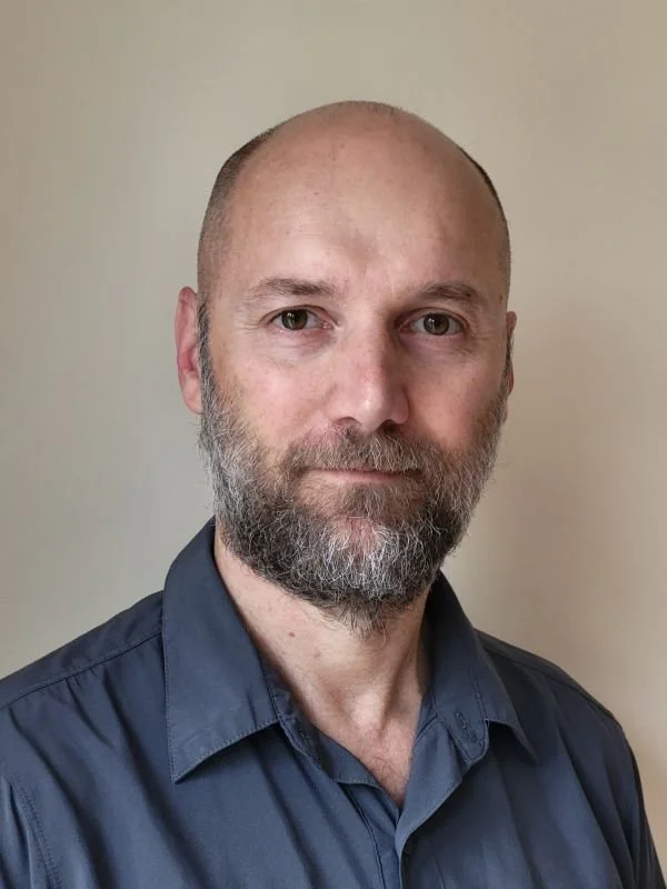
Eng. Vincenzo Miceli
Enzo is a theoretical physicist from the University of Palermo. He began his semiconductor industry career at STMicroelectronics in1998 before joining Intel Ireland in 2001, dedicating his entire career to advanced lithography. Throughout his tenure at Intel, Enzo has worked extensively within Technology Development in Hillsboro, Oregon across multiple technology nodes. He played an integral role on the scanner process transfer teams responsible for several milestone Intel HVM firsts, including the introduction of the first 193nm "dry" platform, the first 193nm Immersion platform, and high-volume EUV lithography. Throughout his 25-year career with Intel Ireland, Enzo has spent more than 10 years embedded in Intel’s US sites (OR, AZ, NM) driving scanner performance improvements and technology transfers. Enzo currently leads the Lithography Yield Improvement initiative at Fab 34 in Ireland, with a primary focus on advanced overlay/CD control and scanner fleet automation.