Title:
Beauties and Challenges in Rapid and Large-Area Direct Electron Beam
Abstract:
Lithography is the key elemental process for all micro and nano devices. The principle is to dose a critical amount of energy over a thin organic film (aka resist). A common sense in open facilities worldwide, such as the EuroNanoLab Network and the Japanese ARIM-SETI nanotechnology platform, is that (1) Optical Lithography (OL) gives quick but low-resolution patterning, and (2) Electron Beam Lithography (EBL) gives high-resolution but slow patterning. However, there exists a third way: (3) High-throughput large-area Electron Beam Lithography.
Professor Yoshio Mita will share his past 30 years of experience with high-throughput EBL with the EuroNanoLab members in his clear and humorous talk.
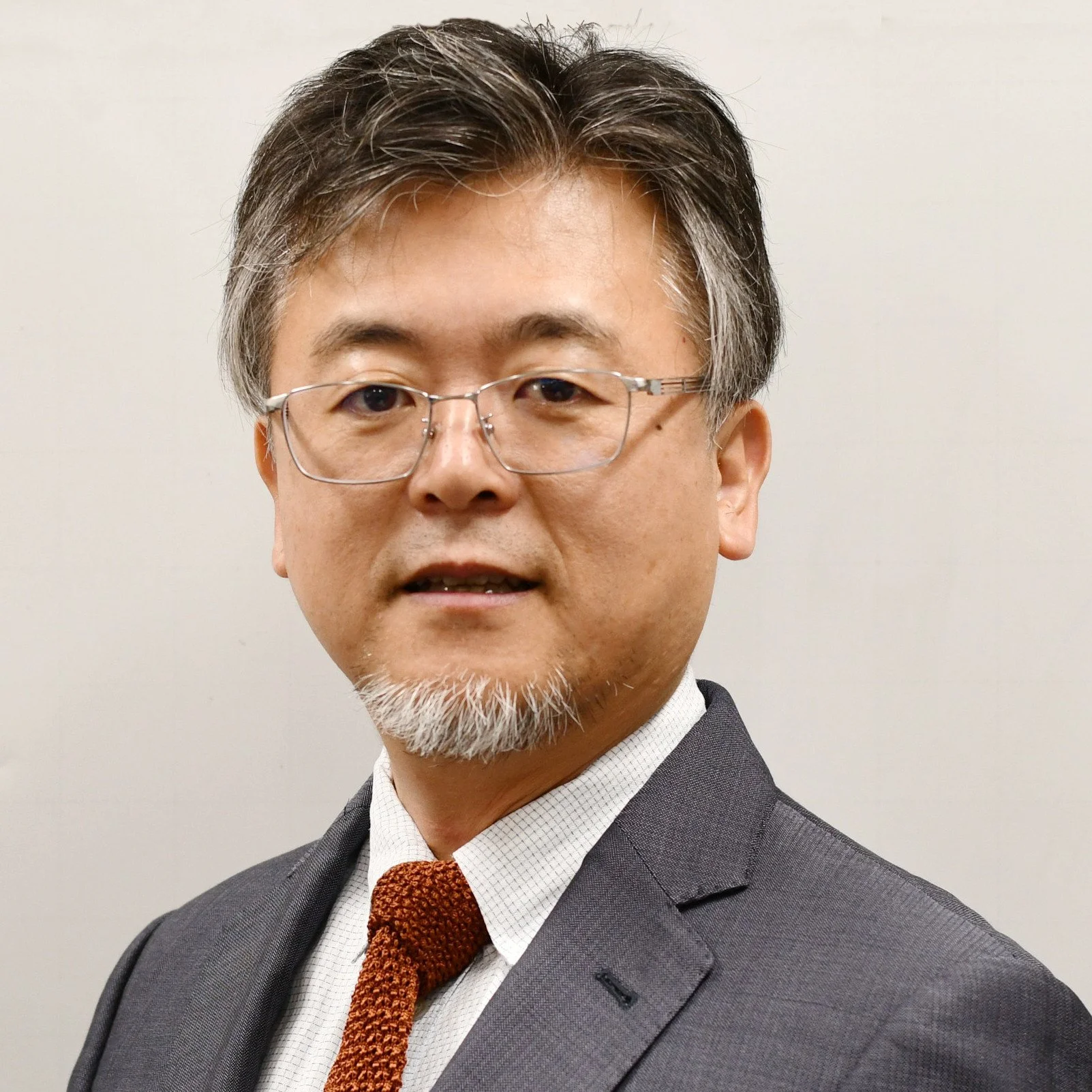
Professor Yoshio Mita
Professor Yoshio Mita is a full professor in the Department of Electrical Engineering and Information Systems (EEIS), Graduate School of Engineering, the University of Tokyo (UTokyo). He serves as the director of the Nanosystem Integration Centre, a gateway centre for collaborative research in micro and nanosystems at the University of Tokyo, as well as a division director of the Platform Device Research Division, Systems Design Lab (d.lab), which manages a world-class supercleanroom open nanotechnology platform. He obtained his BE, ME, and PhD from the Department of Electronic and Electrical Engineering, UTokyo, in 1995, 1997, and 2000, respectively. He was appointed as an assistant professor at the VLSI Design and Education Centre (VDEC, former d.lab) in 2000, and then as a lecturer, associate professor, and full professor at the School of Engineering, UTokyo, in 2001, 2005, and 2022, respectively. His research interests include autonomous distributed microsystems and micro- and nanofabrication technology. The first Best Teaching Award of the School of Engineering at the University of Tokyo was awarded to Pr. Mita in 2013. Prof. Mita is a senior member of IEEE and the Japanese IEE.