About
On behalf of the Organising Committee, it is a great pleasure to welcome you to the 13th Joint EuroSOI Workshop and International Conference on Ultimate Integration on Silicon (EuroSOI-ULIS 2027), which will be held from May 31 to June 4, 2027, at the INL - International Iberian Nanotechnology Laboratory, Braga, Portugal.
The Joint EuroSOI-ULIS International Conference is an annual event that has been running since 2013. Past conferences in this series have been held in Athens, Greece (2017); Granada, Spain (2018); Grenoble, France (2019); Caen, France (virtual, 2020); Caen, France (2021); Udine, Italy (2022); Tarragona, Spain (2023); Athens, Greece (2024); Warsaw, Poland (2025); and Granada, Spain (2026). This year, the conference will be held in Braga, Portugal.
This conference aims to bring together scientists and engineers in an interactive forum to discuss SOI technology and advanced microelectronic devices. A key objective is to foster collaboration and partnerships among academia, research institutions, and industry stakeholders.
We warmly invite students and researchers from both academic and industrial backgrounds to submit their abstracts and join us in Braga. The conference offers a valuable opportunity to engage with colleagues, share knowledge, and experience the charm of this marvellous city.
Satellite events
-
Monday 31 May (afternoon) – Tuesday 1 June 2027
A 1,5-day workshop held ahead of the main conference. Programme details will follow.
Title: Semiconductor Technology Roadmaps and International Cooperation: Aligning European Priorities with Global Innovation TrendsAbstract:
The semiconductor landscape is evolving rapidly under the influence of technological innovation, industrial policy, and geopolitical developments. This workshop will share the first results from the ICOS² project and gather perspectives from international experts on national semiconductor strategies, emerging technologies, and roadmap priorities.
Discussions will focus on benchmarking European activities against global trends, identifying strategic gaps and complementarities, and exploring opportunities for future international research and innovation partnerships.
-
Tuesday 1 June 2027, 16h-19h30
Title: From R&D Nodes to Innovation Networks: Integrating Europe's Semiconductor Capabilities into a Competitive AdvantageAbstract:
The ability to connect people, knowledge, technologies, infrastructures, markets, and capital is often what turns individual capabilities into economic and societal value.
This session will bring together organisations and initiatives that help connect Europe's semiconductor ecosystem, including Chips Competence Centres, the European Chip Design Platform, Pilot Lines, research infrastructure networks, and policymakers. It will explore how these initiatives can translate Europe's semiconductor capabilities into greater economic and societal value, competitiveness, resilience, and technological autonomy.
The event will comprise two parts:
Part I – Information Session: An overview of the different European initiatives, the capabilities and opportunities they provide, and how researchers, start-ups, SMEs, and industry can access them.
Part II – Broader Impact Session: A round-table discussion examining how these initiatives contribute to building a stronger European semiconductor ecosystem, what makes them successful, what impact they have generated so far, and what could be improved.
Conference Topics
High-quality contributions are solicited in the following areas:
Advanced SOI and emerging semiconductor materials, including strained Si/Ge, III–V and oxide semiconductors, carbon nanotubes, graphene and other 2D materials, van der Waals heterostructures, ultra-thin films, buried oxides, defects, interfaces and advanced gate dielectrics.
Advanced transistor architectures and Beyond-CMOS devices, including FD-SOI, FinFETs, nanowires, nanosheets, CFETs, MuGFETs, vertical MOSFETs, FeFETs, TFETs, 2D-semiconductor transistors, MEMS/NEMS and related concepts.
More-than-Moore and functional devices, including nanoelectronics and biosensors, bioelectronics, RF devices, flexible electronics, imagers, integrated photonics, 2D optoelectronics, energy harvesting, quantum and cryogenic devices, nanofluidic and iontronic devices.
3D and heterogeneous integration, including monolithic and heterogeneous device integration, 2D materials on CMOS and photonic platforms, and emerging integration schemes.
Transport, modelling and simulation, including electronic and ionic transport, compact modelling, atomistic and multiscale approaches, machine-learning-assisted modelling, device/process simulation and DTCO.
CMOS scaling and device/circuit performance, including transistor, switch and memory scaling, performance benchmarking and device- and circuit-level evaluation.
Advanced characterisation, reliability and variability, including test structures, operando and advanced characterisation techniques, interface/defect analysis, parameter extraction, reliability and variability of emerging materials and devices.
Emerging memory technologies, including memristors and 2D-based memories, ferroelectric and other novel memory devices.
Neuromorphic and unconventional computing hardware, including in-memory and in-sensor computing, neuromorphic systems, quantum computing architectures and other emerging computing paradigms.
Call for papers
How to submit
Original abstracts (2 pages, including illustrations) will be reviewed by the Scientific Committee. Selected conference contributions are expected to be considered for publication in a Special Issue of Elsevier’s Solid-State Electronics. The Special Issue will follow the format of previous editions, with extended conference contributions typically limited to 4 pages and flexibility for up to 5 pages where necessary.
The Special Issue will also welcome original research articles within the scope of the conference, which should follow the journal's standard submission requirements. Further details on the submission requirements will be announced in due course.
Awards
Important dates
| Abstract submission deadline | |
|---|---|
| Notification of acceptance | To be announced |
| Registration opening | To be announced |
| 4-page paper submission (SSE) | To be announced |
| Satellite events | – |
| Main conference | – |
Androula Nassiopoulou Best Paper Award: Awarded by the SiNANO Institute.
Best Poster Award: Awarded by Elsevier's Solid-State Electronics journal.
Sponsors

Venue
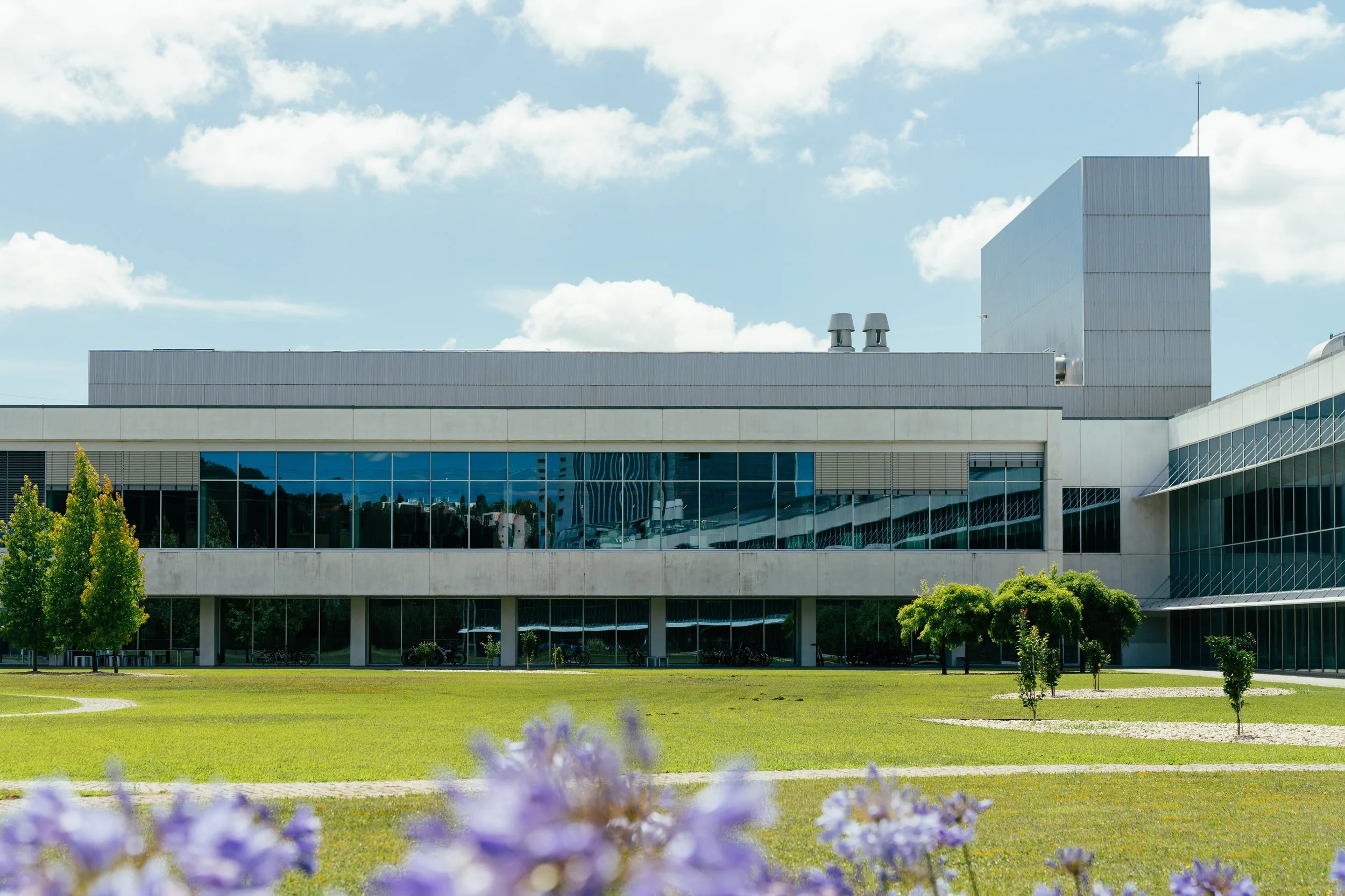
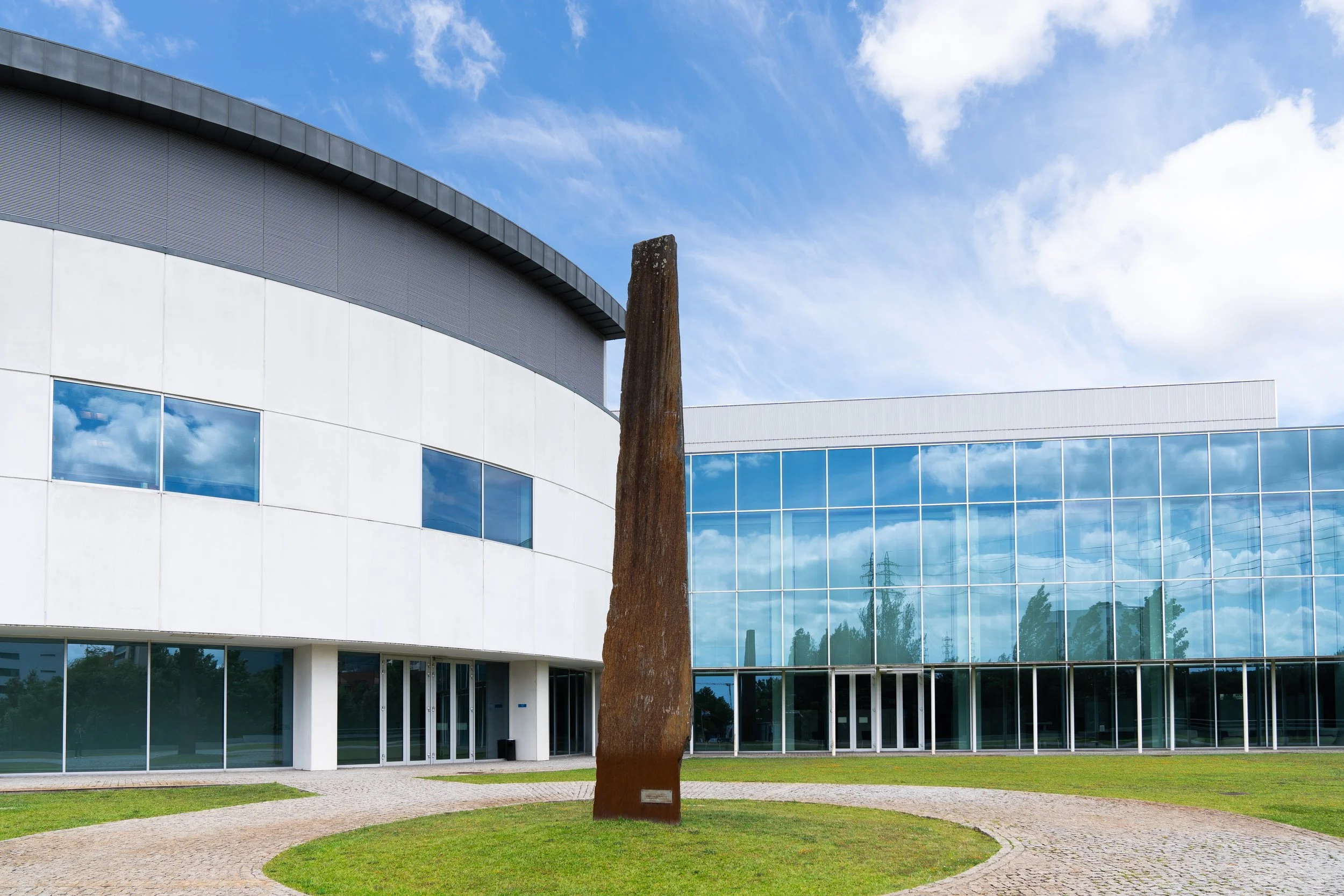


The INL International Iberian Nanotechnology Laboratory, located in Braga (North of Portugal), was founded by the governments of Portugal and Spain under an international legal framework to perform interdisciplinary research and deploy and articulate nanotechnology for the benefit of society.
INL aims to become the worldwide hub for nanotechnology, addressing society’s grand challenges.
INL – International Iberian Nanotechnology Laboratory
Av. Mestre José Veiga
4715-330 Braga | Portugal